Researchers study mechanisms that limit electron mobility in semiconductors

Recent advancements in understanding electron scattering mechanisms within semiconductors may lead to more efficient electronic devices. Researchers at the Jawaharlal Nehru Centre for Advanced Scientific Research (JNCASR) in India have explored the factors limiting electron mobility, focusing heavily on Scandium Nitride (ScN), a promising material for future electronics due to its robust electronic properties and high thermal stability.
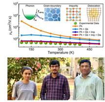
The study indicates that while the fundamental interactions between electrons and phonons impose an upper limit on the mobility of ScN, additional factors like ionized impurities and grain boundaries significantly hinder this mobility. By eliminating these factors—especially impurities and defects in crystal structure—researchers believe it is possible to enhance the performance of ScN in practical applications.
The findings regarding electron scattering in semiconductors not only enhance the understanding of material science but also pave the way for innovative electronic devices that meet the increasing demands for speed and efficiency. Future work will likely refine these insights, potentially leading to novel applications in the fast-evolving tech landscape. The ongoing research signifies a breakthrough moment for both academic and industrial sectors interested in advancing semiconductor functionality.


